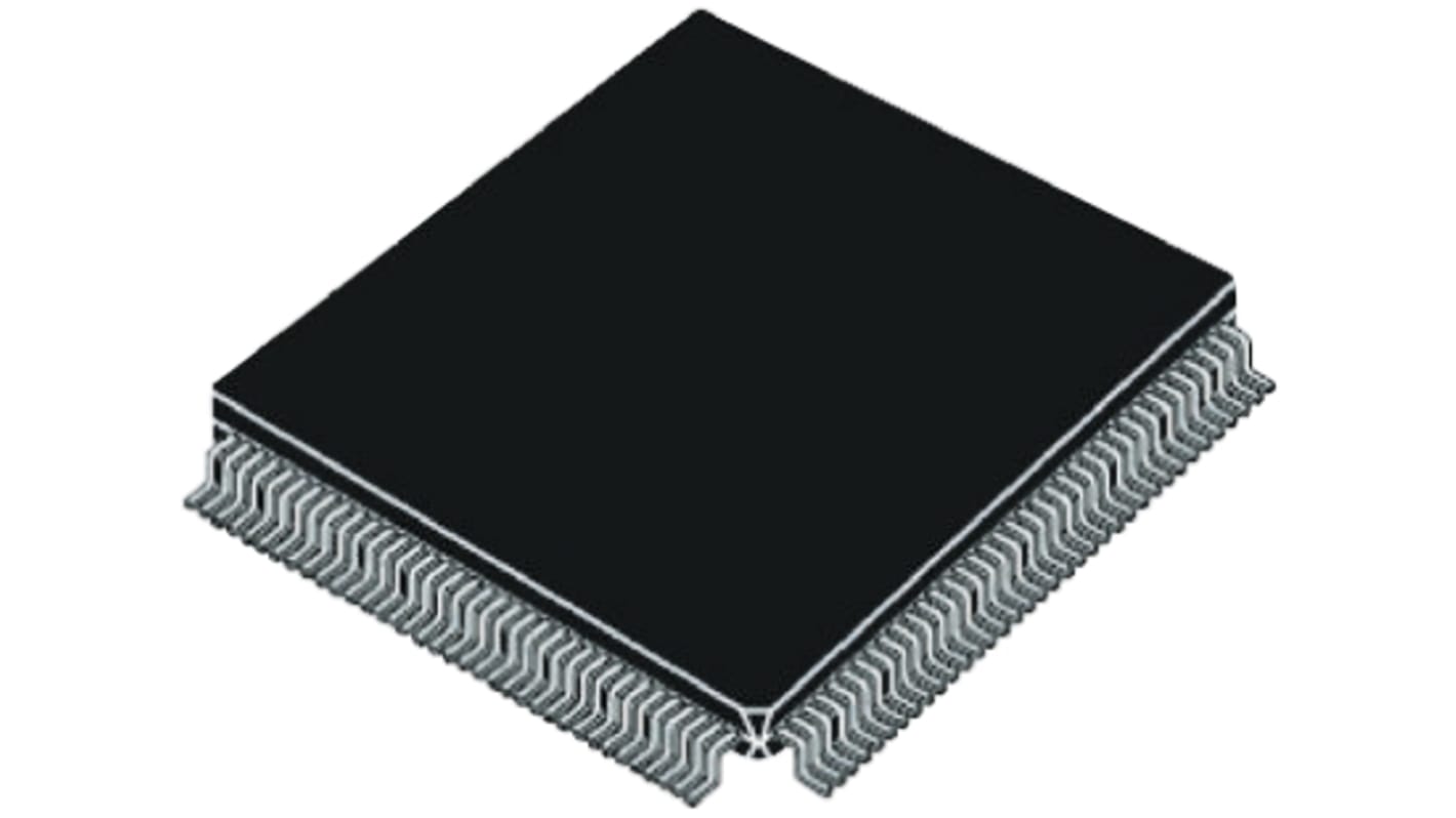
Lattice FPGA iCE40HX4K-TQ144 iCE40 3520 Cells, 80000 bit 440 Blocks, 144-Pin TQFP
- RS-stocknr.:
- 772-0057
- Fabrikantnummer:
- iCE40HX4K-TQ144
- Fabrikant:
- Lattice Semiconductor

Subtotaal (1 eenheid)*
€ 9,19
(excl. BTW)
€ 11,12
(incl. BTW)
GRATIS bezorging voor bestellingen vanaf € 90,00
Op voorraad
- Plus verzending 10 stuk(s) vanaf 13 juli 2026
- Plus verzending 450 stuk(s) vanaf 20 juli 2026
Heeft u meer nodig? Klik op 'Controleer leverdata' voor extra voorraad en levertijden.
Aantal stuks | Per stuk |
|---|---|
| 1 + | € 9,19 |
*prijsindicatie
- RS-stocknr.:
- 772-0057
- Fabrikantnummer:
- iCE40HX4K-TQ144
- Fabrikant:
- Lattice Semiconductor
Specificaties
Datasheets
Wetgeving en conformiteit
Productomschrijving
Zoek vergelijkbare producten door een of meer kenmerken te selecteren.
Alles selecteren | Attribuut | Waarde |
|---|---|---|
| Merk | Lattice Semiconductor | |
| Series | iCE40 | |
| Product Type | FPGA | |
| Number of Logic Cells | 3520 | |
| Number of Logic Units | 440 | |
| Number of Registers | 3520 | |
| Mount Type | Surface | |
| Package Type | TQFP | |
| Minimum Supply Voltage | 1.14V | |
| Maximum Supply Voltage | 1.26V | |
| Pin Count | 144 | |
| Minimum Operating Temperature | -40°C | |
| Number of RAM Bits | 80000bit | |
| Maximum Operating Temperature | 85°C | |
| Height | 1.45mm | |
| Length | 20mm | |
| Standards/Approvals | No | |
| Automotive Standard | No | |
| Alles selecteren | ||
|---|---|---|
Merk Lattice Semiconductor | ||
Series iCE40 | ||
Product Type FPGA | ||
Number of Logic Cells 3520 | ||
Number of Logic Units 440 | ||
Number of Registers 3520 | ||
Mount Type Surface | ||
Package Type TQFP | ||
Minimum Supply Voltage 1.14V | ||
Maximum Supply Voltage 1.26V | ||
Pin Count 144 | ||
Minimum Operating Temperature -40°C | ||
Number of RAM Bits 80000bit | ||
Maximum Operating Temperature 85°C | ||
Height 1.45mm | ||
Length 20mm | ||
Standards/Approvals No | ||
Automotive Standard No | ||
Field Programmable Gate Arrays, Lattice Semiconductor
An FPGA is a semiconductor device consisting of a Matrix of Configurable Logic Blocks (CLBs) connected through programmable interconnects. The user determines these interconnections by programming SRAM. A CLB can be simple (AND, OR gates, etc) or complex (a Block of RAM). The FPGA allows changes to be MADE to a design even after the device is soldered into a PCB.
Gerelateerde Links
- Lattice FPGA iCE40 3520 Cells, 80000 bit 440 Blocks, 144-Pin TQFP
- Lattice FPGA iCE40 1280 Cells, 64000 bit 160 Blocks, 100-Pin VQFP
- Lattice FPGA iCE40HX1K-VQ100 iCE40 1280 Cells, 64000 bit 160 Blocks, 100-Pin VQFP
- Lattice FPGA iCE40 LP/HX 1280 Cells, 64 kB 160 Blocks, 49-Pin UCBGA
- Lattice FPGA iCE40LP1K-CM49 iCE40 LP/HX 1280 Cells, 64 kB 160 Blocks, 49-Pin UCBGA
- Altera FPGA Cyclone II 4608 Cells, 4608 Blocks, 144-Pin TQFP
- Altera FPGA EP2C5T144C8N Cyclone II 4608 Cells, 4608 Blocks, 144-Pin TQFP
- Altera FPGA EP2C5T144I8N Cyclone II 4608 Cells, 4608 Blocks, 144-Pin TQFP