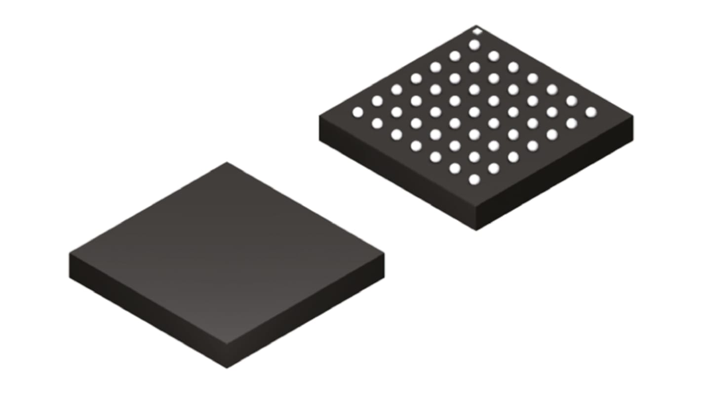
Lattice FPGA iCE40LP1K-CM49, iCE40 LP 1280 Cells, 64kbit, 160 Blocks, 49-Pin UCBGA
- RS-stocknr.:
- 772-0085P
- Fabrikantnummer:
- iCE40LP1K-CM49
- Fabrikant:
- Lattice Semiconductor

Subtotaal 1 eenheid (geleverd op een tray)*
€ 3,94
(excl. BTW)
€ 4,77
(incl. BTW)
GRATIS bezorging voor bestellingen vanaf € 75,00
Laatste voorraad RS
- Laatste 63 stuk(s), klaar voor verzending vanaf een andere locatie
Aantal stuks | Per stuk |
|---|---|
| 1 + | € 3,94 |
*prijsindicatie
- RS-stocknr.:
- 772-0085P
- Fabrikantnummer:
- iCE40LP1K-CM49
- Fabrikant:
- Lattice Semiconductor
Specificaties
Datasheets
Wetgeving en conformiteit
Productomschrijving
Zoek vergelijkbare producten door een of meer kenmerken te selecteren.
Alles selecteren | Attribuut | Waarde |
|---|---|---|
| Merk | Lattice Semiconductor | |
| Family Name | iCE40 LP | |
| Number of Logic Cells | 1280 | |
| Number of Logic Units | 160 | |
| Number of Registers | 1280 | |
| Mounting Type | Surface Mount | |
| Package Type | UCBGA | |
| Pin Count | 49 | |
| Number of RAM Bits | 64kbit | |
| Dimensions | 3 x 3 x 0.9mm | |
| Height | 0.9mm | |
| Length | 3mm | |
| Minimum Operating Temperature | -40 °C | |
| Maximum Operating Supply Voltage | 1.26 V | |
| Width | 3mm | |
| Minimum Operating Supply Voltage | 1.14 V | |
| Maximum Operating Temperature | +85 °C | |
| Alles selecteren | ||
|---|---|---|
Merk Lattice Semiconductor | ||
Family Name iCE40 LP | ||
Number of Logic Cells 1280 | ||
Number of Logic Units 160 | ||
Number of Registers 1280 | ||
Mounting Type Surface Mount | ||
Package Type UCBGA | ||
Pin Count 49 | ||
Number of RAM Bits 64kbit | ||
Dimensions 3 x 3 x 0.9mm | ||
Height 0.9mm | ||
Length 3mm | ||
Minimum Operating Temperature -40 °C | ||
Maximum Operating Supply Voltage 1.26 V | ||
Width 3mm | ||
Minimum Operating Supply Voltage 1.14 V | ||
Maximum Operating Temperature +85 °C | ||
Field Programmable Gate Arrays, Lattice Semiconductor
An FPGA is a semiconductor device consisting of a matrix of Configurable Logic Blocks (CLBs) connected through programmable interconnects. The user determines these interconnections by programming SRAM. A CLB can be simple (AND, OR gates, etc) or complex (a block of RAM). The FPGA allows changes to be made to a design even after the device is soldered into a PCB.
Gerelateerde Links
- Lattice FPGA iCE40LP1K-CM49, iCE40 LP 1280 Cells, 64kbit, 160 Blocks, 49-Pin UCBGA
- Lattice FPGA iCE40HX1K-VQ100, iCE40 HX 1280 Cells, 64kbit, 160 Blocks, 100-Pin VQFP
- Lattice FPGA ICE40HX4K-TQ144, iCE40 HX 3520 Cells, 80kbit, 440 Blocks, 144-Pin TQFP
- Microchip FPGA MPF300T-1FCG784E, PolarFire FPGA 300000 Cells, 20600kbit, 784-Pin BGA
- Microchip FPGA MPF100TL-FCVG484I, PolarFire FPGA 109000 Cells, 7600kbit, 484-Pin BGA
- Microchip FPGA MPF100TLS-FCG484I, PolarFire FPGA 109000 Cells, 7600kbit, 484-Pin BGA
- Microchip FPGA MPF100TLS-FCVG484I, PolarFire FPGA 109000 Cells, 7600kbit, 484-Pin BGA
- Microchip FPGA MPF100TL-FCSG325E, PolarFire FPGA 109000 Cells, 7600kbit, 325-Pin TFBGA