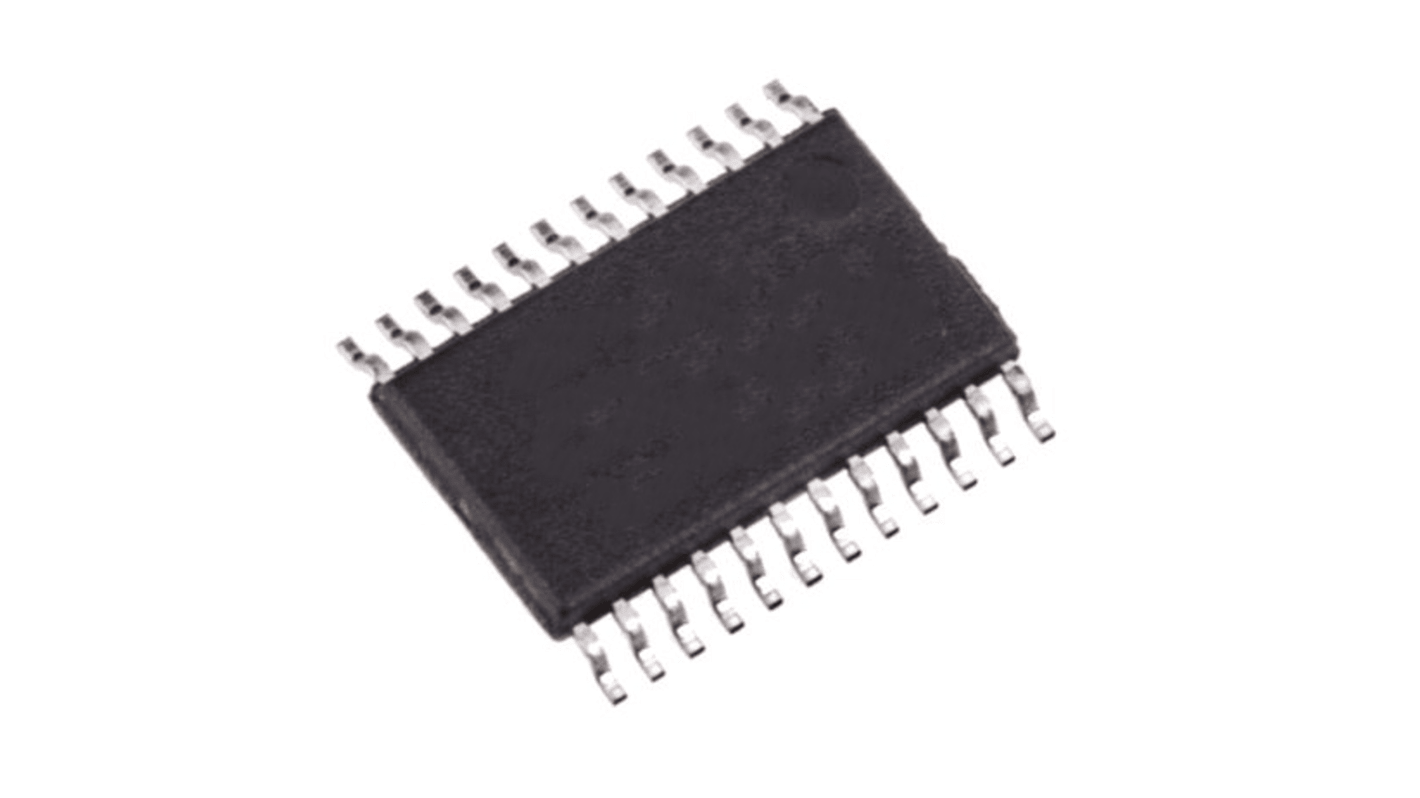
Renesas Electronics 5V2310PGGI Clock Buffer 24-Pin TSSOP
- RS-stocknr.:
- 254-4946
- Fabrikantnummer:
- 5V2310PGGI
- Fabrikant:
- Renesas Electronics

Subtotaal (1 tube van 62 eenheden)*
€ 142,29
(excl. BTW)
€ 172,174
(incl. BTW)
GRATIS bezorging voor bestellingen vanaf € 75,00
Op voorraad
- Plus verzending 186 stuk(s) vanaf 19 januari 2026
Heeft u meer nodig? Klik op 'Controleer leverdata' voor extra voorraad en levertijden.
Aantal stuks | Per stuk | Per tube* |
|---|---|---|
| 62 + | € 2,295 | € 142,29 |
*prijsindicatie
- RS-stocknr.:
- 254-4946
- Fabrikantnummer:
- 5V2310PGGI
- Fabrikant:
- Renesas Electronics
Specificaties
Datasheets
Wetgeving en conformiteit
Productomschrijving
Zoek vergelijkbare producten door een of meer kenmerken te selecteren.
Alles selecteren | Attribuut | Waarde |
|---|---|---|
| Merk | Renesas Electronics | |
| Number of Elements per Chip | 10 | |
| Maximum Supply Current | 50 mA | |
| Maximum Input Frequency | 200MHz | |
| Mounting Type | Surface Mount | |
| Package Type | TSSOP | |
| Pin Count | 24 | |
| Alles selecteren | ||
|---|---|---|
Merk Renesas Electronics | ||
Number of Elements per Chip 10 | ||
Maximum Supply Current 50 mA | ||
Maximum Input Frequency 200MHz | ||
Mounting Type Surface Mount | ||
Package Type TSSOP | ||
Pin Count 24 | ||
The Renesas Electronics high performance, low skew clock buffer that operates up to 200MHz. Two banks of five outputs each provide low skew copies of CLK. Through the use of control pins 1G and 2G, the outputs of banks 1Y(0:4) and 2Y(0:4) can be placed in a low state regardless of CLK input. The device operates in 2.5V and 3.3V environments. The built-in output enable glitch suppression ensures a synchronized output enable sequence to distribute full period clock signals. The IDT5V2310 is characterized for operation from -40°C to +85°C.
High performance 1:10 clock driver for general purpose applications
Pin-to-pin skew < 100 ps
VDD range is 2.3 V to 3.6 V
Output enable glitch suppression
Distributes one clock input to two banks of five outputs
25 Ω on-chip series dampening resistors
Available in TSSOP package
Pin-to-pin skew < 100 ps
VDD range is 2.3 V to 3.6 V
Output enable glitch suppression
Distributes one clock input to two banks of five outputs
25 Ω on-chip series dampening resistors
Available in TSSOP package
Gerelateerde Links
- Renesas Electronics 5V2310PGGI Clock Buffer 24-Pin TSSOP
- Renesas Electronics 5PB1110PGGI Clock Buffer 20-Pin TSSOP
- Renesas Electronics 9DBL411BGILF Clock Buffer 20-Pin TSSOP
- Renesas Electronics 9DB403DGLF Clock Buffer 28-Pin TSSOP
- Renesas Electronics 9DB803DGLF Clock Buffer 48-Pin TSSOP
- Renesas Electronics 5PB1108PGGK Clock Buffer 16-Pin TSSOP
- Renesas Electronics 9DB633AGILF Clock Buffer 28-Pin TSSOP
- Renesas Electronics 9DB233AGILF Clock Buffer 20-Pin TSSOP