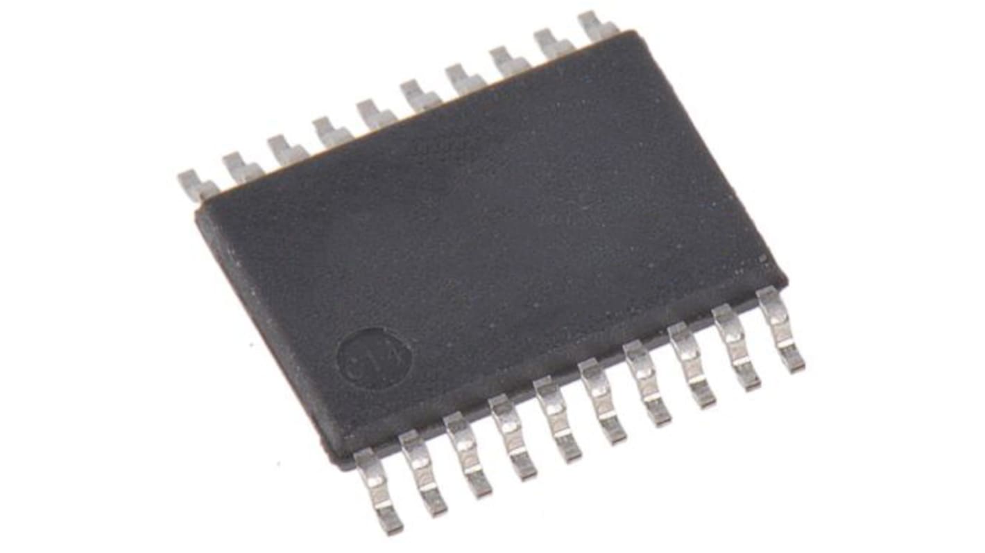
Renesas Electronics 85314BGI-01LF Buffer 20-Pin TSSOP
- RS-stocknr.:
- 250-3469
- Fabrikantnummer:
- 85314BGI-01LF
- Fabrikant:
- Renesas Electronics

Informatie over voorraden is momenteel niet toegankelijk
- RS-stocknr.:
- 250-3469
- Fabrikantnummer:
- 85314BGI-01LF
- Fabrikant:
- Renesas Electronics
Specificaties
Datasheets
Wetgeving en conformiteit
Productomschrijving
Zoek vergelijkbare producten door een of meer kenmerken te selecteren.
Alles selecteren | Attribuut | Waarde |
|---|---|---|
| Merk | Renesas Electronics | |
| Product Type | Buffer | |
| Mount Type | Surface | |
| Maximum Propagation Delay Time | 1.8ns | |
| Package Type | TSSOP | |
| Pin Count | 20 | |
| Minimum Supply Voltage | 2.38V | |
| Maximum Supply Voltage | 3.8V | |
| Minimum Operating Temperature | -40°C | |
| Maximum Operating Temperature | 85°C | |
| Standards/Approvals | RoHS | |
| Length | 13mm | |
| Height | 2.65mm | |
| Automotive Standard | No | |
| Alles selecteren | ||
|---|---|---|
Merk Renesas Electronics | ||
Product Type Buffer | ||
Mount Type Surface | ||
Maximum Propagation Delay Time 1.8ns | ||
Package Type TSSOP | ||
Pin Count 20 | ||
Minimum Supply Voltage 2.38V | ||
Maximum Supply Voltage 3.8V | ||
Minimum Operating Temperature -40°C | ||
Maximum Operating Temperature 85°C | ||
Standards/Approvals RoHS | ||
Length 13mm | ||
Height 2.65mm | ||
Automotive Standard No | ||
The Renesas Electronics fan out buffer is of low skew, high performance 1 to 5 Differential to 2.5V/3.3V LVPECL .It has two selectable clock inputs. The CLK0,nCLK0 pair can accept most standard differential input levels. The single-ended CLK1 can accept LVCMOS or LVTTL input levels. The clock enable is internally synchronized to eliminate runt clock pulses on the outputs during asynchronous assertion/desertion of the clock enable pin.
It has 5 differential 2.5 or 3.3V LVPECL outputs
Selectable differential CLK0/nCLK0 /LVCMOS inputs provided
Maximum output frequency is 700MHz
Translates any single-ended input signal to 3.3V LVPECL levels with resistor bias on nCLK input
Maximum part to part skew is 350ps
It has maximum propagation delay of 1.8ns
RMS phase jitter of 155.52MHz
Ambient operating temperature is -40°C to 85°C
Gerelateerde Links
- Renesas Electronics 85314BGI-01LF Buffer 20-Pin TSSOP
- Renesas Electronics 8535AGI-01LF Buffer 20-Pin TSSOP
- Renesas Electronics 557M-01LF Clock Generator, 20-Pin 2 TSSOP
- Renesas Electronics Clock Buffer 20-Pin TSSOP
- Renesas Electronics 853S014AGILF Buffer 20-Pin TSSOP
- Renesas Electronics 9DBL411BGLFT Clock Buffer 20-Pin TSSOP
- Renesas Electronics 9DBL411BGLF Clock Buffer 20-Pin TSSOP
- Renesas Electronics 9DB233AGILF Clock Buffer 20-Pin TSSOP