Infineon SRAM, CY7C1041G-10ZSXI- 4 MB
- RS-stocknr.:
- 273-7349
- Fabrikantnummer:
- CY7C1041G-10ZSXI
- Fabrikant:
- Infineon

Subtotaal (1 tray van 135 eenheden)*
€ 599,40
(excl. BTW)
€ 724,95
(incl. BTW)
GRATIS bezorging voor bestellingen vanaf € 90,00
Tijdelijk niet op voorraad
- Verzending vanaf 12 november 2026
Heeft u meer nodig? Klik op 'Controleer leverdata' voor extra voorraad en levertijden.
Aantal stuks | Per stuk | Per tray* |
|---|---|---|
| 135 + | € 4,44 | € 599,40 |
*prijsindicatie
- RS-stocknr.:
- 273-7349
- Fabrikantnummer:
- CY7C1041G-10ZSXI
- Fabrikant:
- Infineon
Specificaties
Datasheets
Wetgeving en conformiteit
Productomschrijving
Zoek vergelijkbare producten door een of meer kenmerken te selecteren.
Alles selecteren | Attribuut | Waarde |
|---|---|---|
| Merk | Infineon | |
| Product Type | SRAM | |
| Memory Size | 4MB | |
| Organisation | 256 K x 16 | |
| Number of Words | 256K | |
| Number of Bits per Word | 16 | |
| Minimum Supply Voltage | 0.5V | |
| Mount Type | Surface | |
| Maximum Supply Voltage | 0.5V | |
| Minimum Operating Temperature | -40°C | |
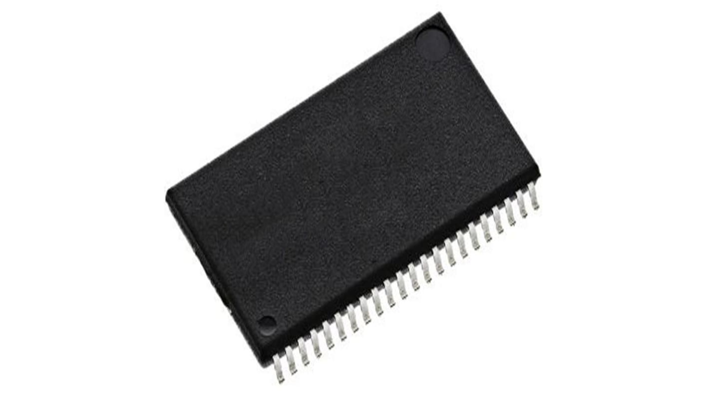
| Package Type | TSOP II | |
| Pin Count | 44 | |
| Maximum Operating Temperature | 85°C | |
| Standards/Approvals | RoHS | |
| Height | 10.26mm | |
| Length | 18.51mm | |
| Width | 1.19mm | |
| Series | CY7C1041G | |
| Supply Current | 45mA | |
| Alles selecteren | ||
|---|---|---|
Merk Infineon | ||
Product Type SRAM | ||
Memory Size 4MB | ||
Organisation 256 K x 16 | ||
Number of Words 256K | ||
Number of Bits per Word 16 | ||
Minimum Supply Voltage 0.5V | ||
Mount Type Surface | ||
Maximum Supply Voltage 0.5V | ||
Minimum Operating Temperature -40°C | ||
Package Type TSOP II | ||
Pin Count 44 | ||
Maximum Operating Temperature 85°C | ||
Standards/Approvals RoHS | ||
Height 10.26mm | ||
Length 18.51mm | ||
Width 1.19mm | ||
Series CY7C1041G | ||
Supply Current 45mA | ||
The Infineon Static RAM are high performance CMOS fast static RAM device with embedded ECC. This Static RAM device offered in single chip enable option and in multiple pin configurations. This device includes an ERR pin that signals an error detection and correction event during a read cycle. Data writes are performed by asserting the chip enable and write enable inputs LOW, while providing the data on IO 0 through IO 15 and address on A0 through A17 pins. The byte high enable and byte low enable inputs control write operations to the upper and lower bytes of the specified memory location.
High speed
Low active and standby currents
1 bit error detection and correction
TTL compatible inputs and outputs
Embedded ECC for single bit error correction