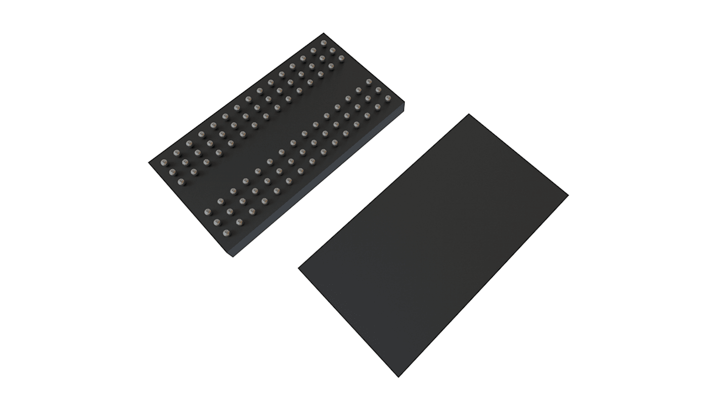
Winbond W9712G6KB25I DDR2 SDRAM 128 MB Surface, 84-Pin 16 bit TFBGA
- RS-stocknr.:
- 188-2730
- Fabrikantnummer:
- W9712G6KB25I
- Fabrikant:
- Winbond

Bulkkorting beschikbaar
Bekijk bulkkortingSubtotaal (1 verpakking van 5 eenheden)*
€ 11,16
(excl. BTW)
€ 13,505
(incl. BTW)
GRATIS bezorging voor bestellingen vanaf € 90,00
Tijdelijk niet op voorraad
- Verzending vanaf 25 november 2026
Heeft u meer nodig? Klik op 'Controleer leverdata' voor extra voorraad en levertijden.
Aantal stuks | Per stuk | Per verpakking* |
|---|---|---|
| 5 - 5 | € 2,232 | € 11,16 |
| 10 - 15 | € 2,03 | € 10,15 |
| 20 - 45 | € 1,992 | € 9,96 |
| 50 - 95 | € 1,968 | € 9,84 |
| 100 + | € 1,766 | € 8,83 |
*prijsindicatie
- RS-stocknr.:
- 188-2730
- Fabrikantnummer:
- W9712G6KB25I
- Fabrikant:
- Winbond
Specificaties
Datasheets
Wetgeving en conformiteit
Productomschrijving
Zoek vergelijkbare producten door een of meer kenmerken te selecteren.
Alles selecteren | Attribuut | Waarde |
|---|---|---|
| Merk | Winbond | |
| Memory Size | 128MB | |
| Product Type | DDR2 SDRAM | |
| Organisation | 16M x 8 bit | |
| Data Bus Width | 16bit | |
| Address Bus Width | 15bit | |
| Number of Bits per Word | 8 | |
| Maximum Random Access Time | 0.4ns | |
| Number of Words | 16M | |
| Mount Type | Surface | |
| Package Type | TFBGA | |
| Pin Count | 84 | |
| Minimum Operating Temperature | -40°C | |
| Maximum Operating Temperature | 95°C | |
| Series | W9712G6KB | |
| Width | 8.1mm | |
| Length | 12.6mm | |
| Height | 0.8mm | |
| Standards/Approvals | RoHS | |
| Minimum Supply Voltage | 1.7V | |
| Supply Current | 135mA | |
| Maximum Supply Voltage | 1.9V | |
| Automotive Standard | No | |
| Alles selecteren | ||
|---|---|---|
Merk Winbond | ||
Memory Size 128MB | ||
Product Type DDR2 SDRAM | ||
Organisation 16M x 8 bit | ||
Data Bus Width 16bit | ||
Address Bus Width 15bit | ||
Number of Bits per Word 8 | ||
Maximum Random Access Time 0.4ns | ||
Number of Words 16M | ||
Mount Type Surface | ||
Package Type TFBGA | ||
Pin Count 84 | ||
Minimum Operating Temperature -40°C | ||
Maximum Operating Temperature 95°C | ||
Series W9712G6KB | ||
Width 8.1mm | ||
Length 12.6mm | ||
Height 0.8mm | ||
Standards/Approvals RoHS | ||
Minimum Supply Voltage 1.7V | ||
Supply Current 135mA | ||
Maximum Supply Voltage 1.9V | ||
Automotive Standard No | ||
The W9712G6KB is a 128M bits DDR2 SDRAM and speed involving -25, 25I and -3.
Double Data Rate architecture: two data transfers per clock cycle
CAS Latency: 3, 4, 5 and 6
Burst Length: 4 and 8
Bi-directional, differential data strobes (DQS and /DQS ) are transmitted / received with data
Edge-aligned with Read data and center-aligned with Write data
DLL aligns DQ and DQS transitions with clock
Differential clock inputs (CLK and /CLK)
Data masks (DM) for write data
Commands entered on each positive CLK edge, data and data mask are referenced to both edges of /DQS
Posted /CAS programmable additive latency supported to make command and data bus efficiency
Read Latency = Additive Latency plus CAS Latency (RL = AL + CL)
Off-Chip-Driver impedance adjustment (OCD) and On-Die-Termination (ODT) for better signal quality
Auto-precharge operation for read and write bursts
Auto Refresh and Self Refresh modes
Precharged Power Down and Active Power Down
Write Data Mask
Write Latency = Read Latency - 1 (WL = RL - 1)
Interface: SSTL_18
Gerelateerde Links
- Winbond DDR2 SDRAM 128 MB Surface, 84-Pin 16 bit TFBGA
- Winbond SDRAM 512 MB Surface, 84-Pin 16 bit VFBGA
- Winbond W9751G6NB25I SDRAM 512 MB Surface, 84-Pin 16 bit VFBGA
- Winbond W9725G6KB-25/TRAY, DDR2 SDRAM Memory 256Mbit Surface Mount, 800MHz, 84-Pin WBGA
- Winbond SDRAM 128 MB Surface, 54-Pin 16 bit TSOP
- Winbond W9812G6KH-6I SDRAM 128 MB Surface, 54-Pin 16 bit TSOP
- Micron MT47H32M16NF-25E:H SDRAM 512 MB Surface Mount, 84-Pin 16 bit TFBGA
- Micron MT47H32M16NF-25E IT:H SDRAM 512 MB Surface Mount, 84-Pin 16 bit TFBGA