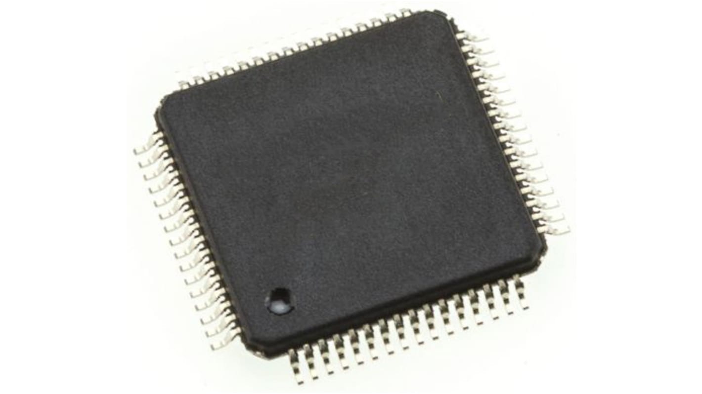
Infineon CY8C4147AZI-S445, 32 bit ARM Cortex M0, PSoC 4100S Plus Microcontroller, 48 MHz, 128kB FLASH, 64-Pin TQFP
- RS-stocknr.:
- 176-9008
- Fabrikantnummer:
- CY8C4147AZI-S445
- Fabrikant:
- Infineon

Subtotaal (1 eenheid)*
€ 4,24
(excl. BTW)
€ 5,13
(incl. BTW)
GRATIS bezorging voor bestellingen vanaf € 90,00
Tijdelijk niet op voorraad
- Verzending vanaf 15 oktober 2026
Heeft u meer nodig? Klik op 'Controleer leverdata' voor extra voorraad en levertijden.
Aantal stuks | Per stuk |
|---|---|
| 1 + | € 4,24 |
*prijsindicatie
- RS-stocknr.:
- 176-9008
- Fabrikantnummer:
- CY8C4147AZI-S445
- Fabrikant:
- Infineon
Specificaties
Datasheets
Wetgeving en conformiteit
Productomschrijving
Zoek vergelijkbare producten door een of meer kenmerken te selecteren.
Alles selecteren | Attribuut | Waarde |
|---|---|---|
| Merk | Infineon | |
| Series | PSoC 4100S Plus | |
| Product Type | Microcontroller | |
| Package Type | TQFP | |
| Mount Type | Surface | |
| Pin Count | 64 | |
| Device Core | ARM Cortex M0 | |
| Data Bus Width | 32bit | |
| Program Memory Size | 128kB | |
| Maximum Clock Frequency | 48MHz | |
| RAM Size | 16kB | |
| Maximum Supply Voltage | 5.5V | |
| Minimum Operating Temperature | -40°C | |
| Maximum Operating Temperature | 85°C | |
| Standards/Approvals | RoHS | |
| Width | 10mm | |
| Number of Programmable I/Os | 54 | |
| Height | 1.4mm | |
| Analogue Comparators | 2 | |
| Length | 10mm | |
| Minimum Supply Voltage | 1.71V | |
| Instruction Set Architecture | Thumb-2 | |
| Automotive Standard | No | |
| ADCs | 2 x 10/12 Bit | |
| Number of Timers | 1 | |
| Program Memory Type | FLASH | |
| Alles selecteren | ||
|---|---|---|
Merk Infineon | ||
Series PSoC 4100S Plus | ||
Product Type Microcontroller | ||
Package Type TQFP | ||
Mount Type Surface | ||
Pin Count 64 | ||
Device Core ARM Cortex M0 | ||
Data Bus Width 32bit | ||
Program Memory Size 128kB | ||
Maximum Clock Frequency 48MHz | ||
RAM Size 16kB | ||
Maximum Supply Voltage 5.5V | ||
Minimum Operating Temperature -40°C | ||
Maximum Operating Temperature 85°C | ||
Standards/Approvals RoHS | ||
Width 10mm | ||
Number of Programmable I/Os 54 | ||
Height 1.4mm | ||
Analogue Comparators 2 | ||
Length 10mm | ||
Minimum Supply Voltage 1.71V | ||
Instruction Set Architecture Thumb-2 | ||
Automotive Standard No | ||
ADCs 2 x 10/12 Bit | ||
Number of Timers 1 | ||
Program Memory Type FLASH | ||
PSoC® 4 is a scalable and reconfigurable platform architecture for a family of programmable embedded system controllers with an Arm® Cortex®-M0 CPU. It combines programmable and reconfigurable analog and digital blocks with flexible automatic routing. The PSoC 4200_BL product family, based on this platform, is a combination of a microcontroller with an integrated Bluetooth Low Energy (BLE), also known as Bluetooth Smart, radio and subsystem (BLESS).
Four opamps with reconfigurable high-drive external and high-bandwidth internal drive, Comparator modes, and ADC input buffering capability Can operate in Deep Sleep mode.
Four programmable logic blocks called universal digital blocks, (UDBs), each with eight macrocells and data path
Cypress-provided peripheral component library, user-defined state machines, and Verilog input
Power Management:
Active mode: 1.7 mA at 3-MHz flash program execution
Deep Sleep mode: 1.5 μA with watch crystal oscillator
Gerelateerde Links
- Infineon, 32 bit ARM Cortex M0, PSoC 4100S Plus Microcontroller, 48 MHz, 128kB FLASH, 64-Pin TQFP
- Infineon CY8C4147AZI-S455, 32 bit ARM Cortex M0 CPU, PSOC 4 Microcontroller, 48 MHz, 128kB FLASH, 64-Pin TQFP
- Infineon, 32 bit ARM Cortex M0 CPU, PSOC 4 Microcontroller, 48 MHz, 128kB FLASH, 64-Pin TQFP
- Infineon CY8C4127AXI-S445, 32 bit ARM Cortex M0 Microcontroller, 24 MHz, 128kB FLASH, 64-Pin TQFP
- Infineon CY8C4147AZI-S475, 32 bit ARM Cortex M0, CY8C4147 Microcontroller, 48 MHz, 128kB FLASH, 64-Pin TQFP
- Infineon, 32 bit ARM Cortex M0 Microcontroller, 24 MHz, 128kB FLASH, 64-Pin TQFP
- Infineon, 32 bit ARM Cortex M0, CY8C4147 Microcontroller, 48 MHz, 128kB FLASH, 64-Pin TQFP
- Infineon, 32 bit ARM Cortex M0 CPU, PSOC 4 Microcontroller, 48 MHz, 128kB FLASH, 48-Pin TQFP