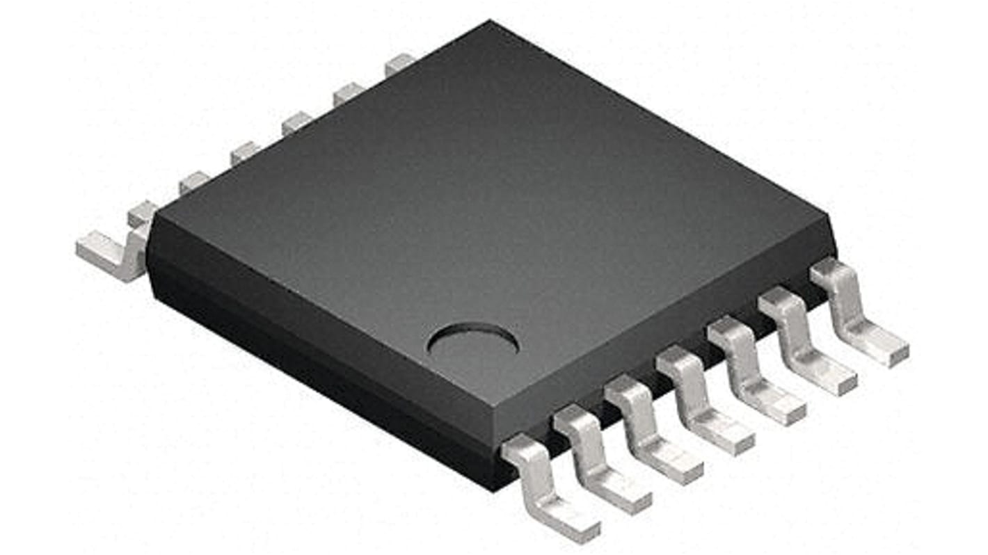
Toshiba 74VHC08FT, Quad 2-Input AND Logic Gate, 14-Pin TSSOP
- RS-stocknr.:
- 171-3594P
- Fabrikantnummer:
- 74VHC08FT
- Fabrikant:
- Toshiba

Subtotaal 50 eenheden (geleverd op een doorlopende strip)*
€ 12,40
(excl. BTW)
€ 15,00
(incl. BTW)
GRATIS bezorging voor bestellingen vanaf € 75,00
Tijdelijk niet op voorraad
- 8.050 stuk(s) klaar voor verzending vanaf een andere locatie
Heeft u meer nodig? Klik op 'Controleer leverdata' voor extra voorraad en levertijden.
Aantal stuks | Per stuk |
|---|---|
| 50 + | € 0,248 |
*prijsindicatie
- RS-stocknr.:
- 171-3594P
- Fabrikantnummer:
- 74VHC08FT
- Fabrikant:
- Toshiba
Specificaties
Datasheets
Wetgeving en conformiteit
Productomschrijving
Zoek vergelijkbare producten door een of meer kenmerken te selecteren.
Alles selecteren | Attribuut | Waarde |
|---|---|---|
| Merk | Toshiba | |
| Logic Function | AND | |
| Mounting Type | Surface Mount | |
| Number of Elements | 4 | |
| Number of Inputs per Gate | 2 | |
| Package Type | TSSOP | |
| Pin Count | 14 | |
| Logic Family | 74VHC | |
| Input Type | CMOS, TTL | |
| Maximum Operating Supply Voltage | 5.5 V | |
| Maximum High Level Output Current | -8mA | |
| Maximum Propagation Delay Time @ Maximum CL | 15.5 ns @ 50 pF | |
| Minimum Operating Supply Voltage | 2 V | |
| Maximum Low Level Output Current | 8mA | |
| Output Type | Buffer, CMOS | |
| Height | 1mm | |
| Propagation Delay Test Condition | 50pF | |
| Automotive Standard | AEC-Q100 | |
| Length | 5mm | |
| Maximum Operating Temperature | +125 °C | |
| Minimum Operating Temperature | -40 °C | |
| Width | 4.4mm | |
| Dimensions | 5 x 4.4 x 1mm | |
| Alles selecteren | ||
|---|---|---|
Merk Toshiba | ||
Logic Function AND | ||
Mounting Type Surface Mount | ||
Number of Elements 4 | ||
Number of Inputs per Gate 2 | ||
Package Type TSSOP | ||
Pin Count 14 | ||
Logic Family 74VHC | ||
Input Type CMOS, TTL | ||
Maximum Operating Supply Voltage 5.5 V | ||
Maximum High Level Output Current -8mA | ||
Maximum Propagation Delay Time @ Maximum CL 15.5 ns @ 50 pF | ||
Minimum Operating Supply Voltage 2 V | ||
Maximum Low Level Output Current 8mA | ||
Output Type Buffer, CMOS | ||
Height 1mm | ||
Propagation Delay Test Condition 50pF | ||
Automotive Standard AEC-Q100 | ||
Length 5mm | ||
Maximum Operating Temperature +125 °C | ||
Minimum Operating Temperature -40 °C | ||
Width 4.4mm | ||
Dimensions 5 x 4.4 x 1mm | ||
The 74VHC08FT is an advanced high speed CMOS 2-INPUT AND GATE fabricated with silicon gate C2MOS technology. It achieves the high speed operation similar to equivalent Bipolar Schottky TTL while maintaining the CMOS low power dissipation. The internal circuit is composed of 4 stages including buffer output, which provide high noise immunity and stable output. An input protection circuit ensures that 0 to 5.5 V can be applied to the input pins without regard to the supply voltage. This device can be used to interface 5 V to 3 V systems and two supply systems such as battery back up. This circuit prevents device destruction due to mismatched supply and input voltages
Wide operating temperature: Topr = -40 to 125
High speed: Propagation delay time = 3.8 ns (typ.) at VCC = 5.0 V
Low power dissipation: ICC = 2.0 μA (max) at Ta = 25
High noise immunity: VNIH = VNIL = 28 % VCC (min)
Power-down protection is provided on all inputs.
Balanced propagation delays: tPLH ≈ tPHL
Wide operating voltage range: VCC(opr) = 2.0 to 5.5 V
Low noise: V = 0.8 V (max)