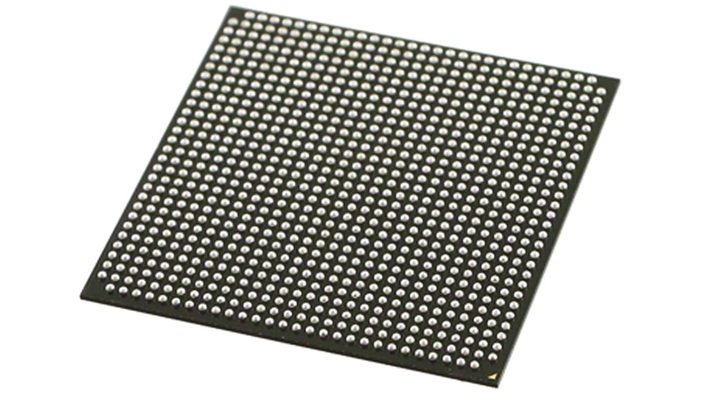
Altera FPGA 5CSXFC5D6F31C8N, Cyclone V SX 85000 Cells, 85000 Gates, 4450K, 32075 Blocks, 896-Pin FBGA
- RS-stocknr.:
- 830-3578
- Fabrikantnummer:
- 5CSXFC5D6F31C8N
- Fabrikant:
- Altera
Bulkkorting beschikbaar
Subtotaal (1 eenheid)*
€ 169,47
(excl. BTW)
€ 205,06
(incl. BTW)
Informatie over voorraden is momenteel niet toegankelijk
Aantal stuks | Per stuk |
|---|---|
| 1 - 9 | € 169,47 |
| 10 - 19 | € 165,13 |
| 20 + | € 161,00 |
*prijsindicatie
- RS-stocknr.:
- 830-3578
- Fabrikantnummer:
- 5CSXFC5D6F31C8N
- Fabrikant:
- Altera
Specificaties
Datasheets
Wetgeving en conformiteit
Productomschrijving
Zoek vergelijkbare producten door een of meer kenmerken te selecteren.
Alles selecteren | Attribuut | Waarde |
|---|---|---|
| Merk | Altera | |
| Family Name | Cyclone V SX | |
| Number of Logic Gates | 85000 | |
| Number of Logic Cells | 85000 | |
| Number of Logic Units | 32075 | |
| Dedicated DSP | Yes | |
| Number of Registers | 128300 | |
| Number of Multipliers | 174 (18 x 18) | |
| Mounting Type | Surface Mount | |
| Package Type | FBGA | |
| Pin Count | 896 | |
| Number of RAM Bits | 4450K | |
| Length | 31mm | |
| Minimum Operating Temperature | 0 °C | |
| Maximum Operating Temperature | +85 °C | |
| Minimum Operating Supply Voltage | 1.07 V | |
| Width | 31mm | |
| Maximum Operating Supply Voltage | 1.13 V | |
| Alles selecteren | ||
|---|---|---|
Merk Altera | ||
Family Name Cyclone V SX | ||
Number of Logic Gates 85000 | ||
Number of Logic Cells 85000 | ||
Number of Logic Units 32075 | ||
Dedicated DSP Yes | ||
Number of Registers 128300 | ||
Number of Multipliers 174 (18 x 18) | ||
Mounting Type Surface Mount | ||
Package Type FBGA | ||
Pin Count 896 | ||
Number of RAM Bits 4450K | ||
Length 31mm | ||
Minimum Operating Temperature 0 °C | ||
Maximum Operating Temperature +85 °C | ||
Minimum Operating Supply Voltage 1.07 V | ||
Width 31mm | ||
Maximum Operating Supply Voltage 1.13 V | ||
Cyclone FPGA, Altera
An FPGA is a semiconductor device consisting of a matrix of Configurable Logic Blocks (CLBs) connected through programmable interconnects. The user determines these interconnections by programming SRAM. A CLB can be simple (AND, OR gates, etc) or complex (a block of RAM). The FPGA allows changes to be made to a design even after the device is soldered into a PCB.
Gerelateerde Links
- Altera FPGA EP3C16F484C8N, Cyclone III 15408 Cells, 15408 Blocks, 484-Pin FBGA
- Altera FPGA EP3C55F484C7N, Cyclone III 55856 Cells, 2396160bit, 3491 Blocks, 484-Pin FBGA
- Altera FPGA EP4CGX15BF14C8N, Cyclone IV GX 14400 Cells, 540kbit, 900 Blocks, 169-Pin FBGA
- Altera FPGA EP4CE6F17C8LN, Cyclone 6272 Cells, 6272 Gates, 276480, 392 Blocks, 256-Pin FBGA
- Altera FPGA EP4CE6F17C8N, Cyclone 6272 Cells, 6272 Gates, 276480, 392 Blocks, 256-Pin FBGA
- Altera FPGA EP4CE30F23C8N, Cyclone IV E 28848 Cells, 594kbit, 1803 Blocks, 484-Pin FBGA
- FTDI Chip Morph-IC-II Altera Cyclone-II Module
- Altera FPGA 5CEBA2F17C8N, Cyclone V 25000 Cells, 25000 Gates, 2002944, 9434 Blocks, 256-Pin FBGA
