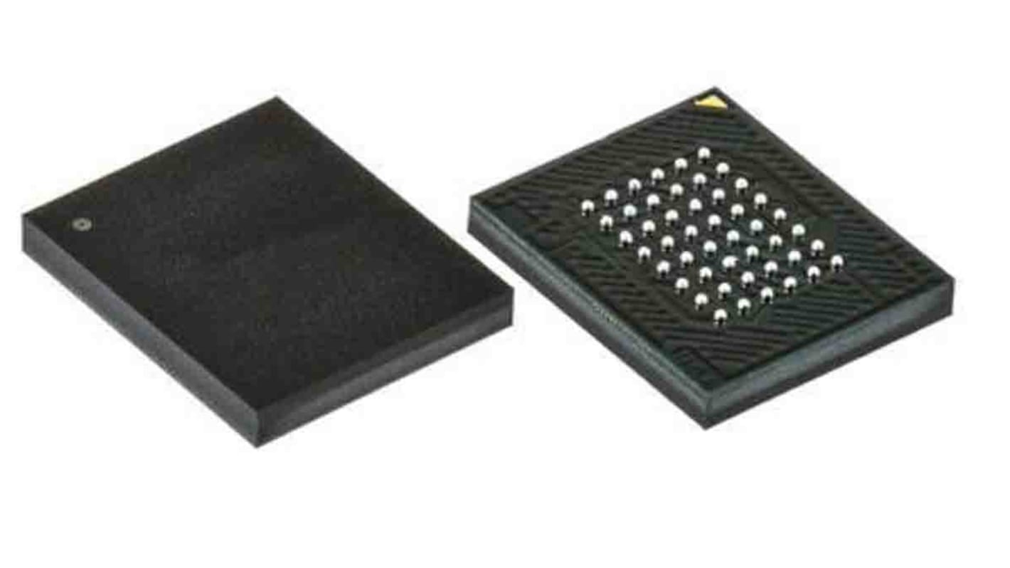
Infineon NOR 64 MB CFI Flash Memory 48-Pin BGA, S29GL064S70BHI030
- RS-stocknr.:
- 193-8826
- Fabrikantnummer:
- S29GL064S70BHI030
- Fabrikant:
- Infineon

Subtotaal (1 verpakking van 5 eenheden)*
€ 17,57
(excl. BTW)
€ 21,26
(incl. BTW)
GRATIS bezorging voor bestellingen vanaf € 90,00
Op voorraad
- Plus verzending 240 stuk(s) vanaf 13 juli 2026
Heeft u meer nodig? Klik op 'Controleer leverdata' voor extra voorraad en levertijden.
Aantal stuks | Per stuk | Per verpakking* |
|---|---|---|
| 5 + | € 3,514 | € 17,57 |
*prijsindicatie
- RS-stocknr.:
- 193-8826
- Fabrikantnummer:
- S29GL064S70BHI030
- Fabrikant:
- Infineon
Specificaties
Datasheets
Wetgeving en conformiteit
Productomschrijving
Zoek vergelijkbare producten door een of meer kenmerken te selecteren.
Alles selecteren | Attribuut | Waarde |
|---|---|---|
| Merk | Infineon | |
| Memory Size | 64MB | |
| Product Type | Flash Memory | |
| Interface Type | CFI | |
| Package Type | BGA | |
| Pin Count | 48 | |
| Organisation | 8M x 8 bit | |
| Mount Type | Surface | |
| Cell Type | NOR | |
| Minimum Supply Voltage | 2.7V | |
| Maximum Supply Voltage | 3.6V | |
| Timing Type | Asynchronous | |
| Minimum Operating Temperature | -40°C | |
| Maximum Operating Temperature | 85°C | |
| Height | 0.84mm | |
| Standards/Approvals | No | |
| Length | 8.15mm | |
| Width | 6.15mm | |
| Number of Bits per Word | 8 | |
| Automotive Standard | AEC-Q100 | |
| Maximum Random Access Time | 70ns | |
| Number of Words | 8K | |
| Supply Current | 50mA | |
| Series | S29GL064S | |
| Alles selecteren | ||
|---|---|---|
Merk Infineon | ||
Memory Size 64MB | ||
Product Type Flash Memory | ||
Interface Type CFI | ||
Package Type BGA | ||
Pin Count 48 | ||
Organisation 8M x 8 bit | ||
Mount Type Surface | ||
Cell Type NOR | ||
Minimum Supply Voltage 2.7V | ||
Maximum Supply Voltage 3.6V | ||
Timing Type Asynchronous | ||
Minimum Operating Temperature -40°C | ||
Maximum Operating Temperature 85°C | ||
Height 0.84mm | ||
Standards/Approvals No | ||
Length 8.15mm | ||
Width 6.15mm | ||
Number of Bits per Word 8 | ||
Automotive Standard AEC-Q100 | ||
Maximum Random Access Time 70ns | ||
Number of Words 8K | ||
Supply Current 50mA | ||
Series S29GL064S | ||
The S29GL-S mid density family of devices are 3.0-volt single-power flash memory manufactured using 65 nm MirrorBit technology.
The S29GL064S is a 64-Mb device organized as 4,194,304 words or 8,388,608 bytes. Depending on the model number, the devices have 16bit wide data bus only, or a 16bit wide data bus that can also function as an 8bit wide data bus by using the BYTE# input.
The devices can be programmed either in the host system or in standard EPROM programmers. Access times as fast as 70 ns are available. Package offerings include 48pin TSOP, 56pin TSOP, 48-ball fine-pitch BGA, and 64-ball Fortified BGA, depending on model number. Each device has separate chip enable (CE#), write enable (WE#) and output enable (OE#) controls. Each device requires only a single 3.0-volt power supply for both read and write functions. In addition to a VCC input, a high-voltage accelerated program (ACC) feature is supported through increased voltage on the WP#/ACC or ACC input. This feature is intended to facilitate system production. Commands are written to the device using standard microprocessor write timing. Write cycles also internally latch addresses and data needed for the programming and erase operations.
The sector erase architecture allows memory sectors to be erased and reprogrammed without affecting the data contents of other sectors. The device is fully erased when shipped from the factory.
The Advanced Sector Protection features several levels of sector protection, which can disable both the program and erase operations in certain sectors.
Gerelateerde Links
- Infineon NOR 64 MB CFI Flash Memory 48-Pin BGA
- Infineon NOR 256 MB CFI Flash Memory 64-Pin BGA
- Infineon NOR 256 MB CFI Flash Memory 64-Pin BGA, S29GL256P11FFIV20
- Infineon NOR 512 MB CFI, SPI Flash Memory 24-Pin BGA
- Infineon NOR 512 MB CFI, SPI Flash Memory 24-Pin BGA, S25FL512SAGBHI310
- Infineon NOR 512 MB CFI, SPI Flash Memory 24-Pin BGA, S25FL512SAGBHID10
- Infineon 512 MB CFI Flash Memory 64-Pin BGA, S29GL512T11FHIV20
- Infineon NOR 8 MB CFI Flash Memory 48-Pin TSOP