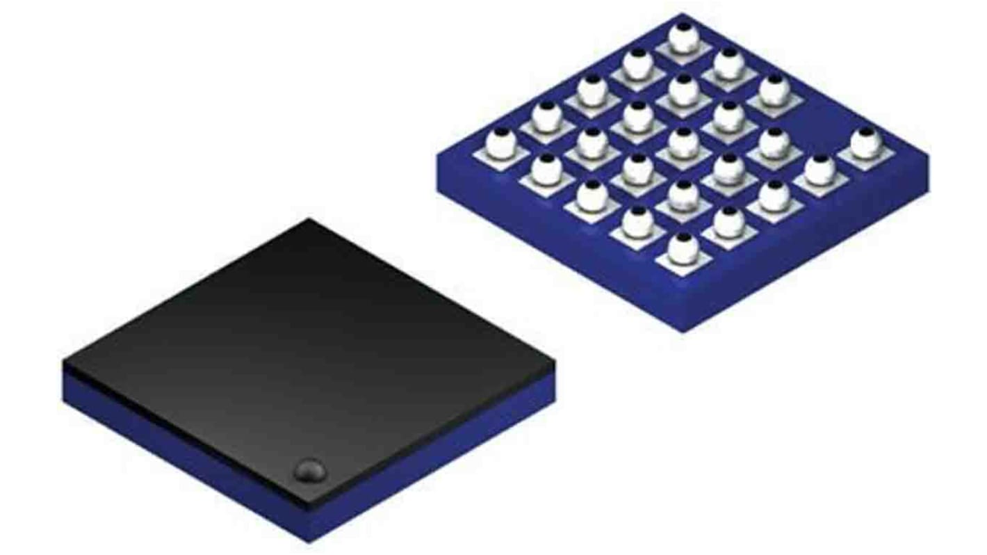
Infineon NOR 256Mbit SPI Flash Memory 24-Pin BGA, S25FL256LAGBHV020
- RS-stocknr.:
- 184-0071P
- Fabrikantnummer:
- S25FL256LAGBHV020
- Fabrikant:
- Infineon

Subtotaal 2 eenheden (geleverd op een tray)*
€ 6,49
(excl. BTW)
€ 7,852
(incl. BTW)
GRATIS bezorging voor bestellingen vanaf € 75,00
Op voorraad
- 1.346 stuk(s) klaar voor verzending vanaf een andere locatie
Heeft u meer nodig? Klik op 'Controleer leverdata' voor extra voorraad en levertijden.
Aantal stuks | Per stuk |
|---|---|
| 2 + | € 3,245 |
*prijsindicatie
- RS-stocknr.:
- 184-0071P
- Fabrikantnummer:
- S25FL256LAGBHV020
- Fabrikant:
- Infineon
Specificaties
Datasheets
Wetgeving en conformiteit
Productomschrijving
Zoek vergelijkbare producten door een of meer kenmerken te selecteren.
Alles selecteren | Attribuut | Waarde |
|---|---|---|
| Merk | Infineon | |
| Memory Size | 256Mbit | |
| Interface Type | SPI | |
| Package Type | BGA | |
| Pin Count | 24 | |
| Organisation | 32M x 8 bit | |
| Mounting Type | Surface Mount | |
| Cell Type | NOR | |
| Minimum Operating Supply Voltage | 2.7 V | |
| Maximum Operating Supply Voltage | 3.6 V | |
| Block Organisation | Symmetrical | |
| Length | 6mm | |
| Height | 0.95mm | |
| Width | 8mm | |
| Dimensions | 8 x 6 x 0.95mm | |
| Series | S25FL | |
| Number of Words | 32M | |
| Minimum Operating Temperature | -40 °C | |
| Number of Bits per Word | 8bit | |
| Maximum Operating Temperature | +105 °C | |
| Automotive Standard | AEC-Q100 | |
| Maximum Random Access Time | 8ns | |
| Alles selecteren | ||
|---|---|---|
Merk Infineon | ||
Memory Size 256Mbit | ||
Interface Type SPI | ||
Package Type BGA | ||
Pin Count 24 | ||
Organisation 32M x 8 bit | ||
Mounting Type Surface Mount | ||
Cell Type NOR | ||
Minimum Operating Supply Voltage 2.7 V | ||
Maximum Operating Supply Voltage 3.6 V | ||
Block Organisation Symmetrical | ||
Length 6mm | ||
Height 0.95mm | ||
Width 8mm | ||
Dimensions 8 x 6 x 0.95mm | ||
Series S25FL | ||
Number of Words 32M | ||
Minimum Operating Temperature -40 °C | ||
Number of Bits per Word 8bit | ||
Maximum Operating Temperature +105 °C | ||
Automotive Standard AEC-Q100 | ||
Maximum Random Access Time 8ns | ||
- Land van herkomst:
- US
Serial Peripheral Interface (SPI) with Multi-I/O
Clock polarity and phase modes 0 and 3
Double Data Rate (DDR) option
Quad peripheral Interface (QPI) option
Extended Addressing: 24- or 32-bit address options
Serial Command subset and footprint compatible with S25FL-A, S25FL1-K, S25FL-P, S25FL-S and S25FS-S SPI families
Multi I/O Command subset and footprint compatible with S25FL-P, S25FL-S and S25FS-S SPI families
Read
Commands: Normal, Fast, Dual I/O, Quad I/O, DualO,QuadO, DDR Quad I/O.
Modes: Burst Wrap, Continuous (XIP), QPI
Serial Flash Discoverable Parameters (SFDP) for configuration information.
Program Architecture
256 Bytes Page Programming buffer
3.0 V FL-L Flash Memory
Program suspend and resume
Erase Architecture
Uniform 4 KB Sector Erase
Uniform 32 KB Half Block Erase
Uniform 64 KB Block Erase
Chip erase
Erase suspend and resume
100,000 Program/Erase Cycles, minimum
20 Year Data Retention, minimum
Security features
Status and Configuration Register Protection
Four Security Regions of 256 bytes each outside the main
Flash array
Legacy Block Protection: Block range
Individual and Region Protection
Individual Block Lock: Volatile individual Sector/Block
Pointer Region: Non-Volatile Sector/Block range
Power Supply Lock-down, Password, or Permanent protection of Security Regions 2 and 3 and Pointer Region
Technology
65 nm Floating Gate Technology
Single Supply Voltage with CMOS I/O
2.7 V to 3.6 V
Packages (all Pb-free)
8-pin SOIC 208 mil (SOC008) — S25FL128L only
WSON 5 x 6 mm (WND008) — S25FL128L only
WSON 6 x 8 mm (WNG008) — S25FL256L only
16-pin SOIC 300 mil (SO3016)
BGA-24 6 x 8 mm
5 x 5 ball (FAB024) footprint
4 x 6 ball (FAC024) footprint