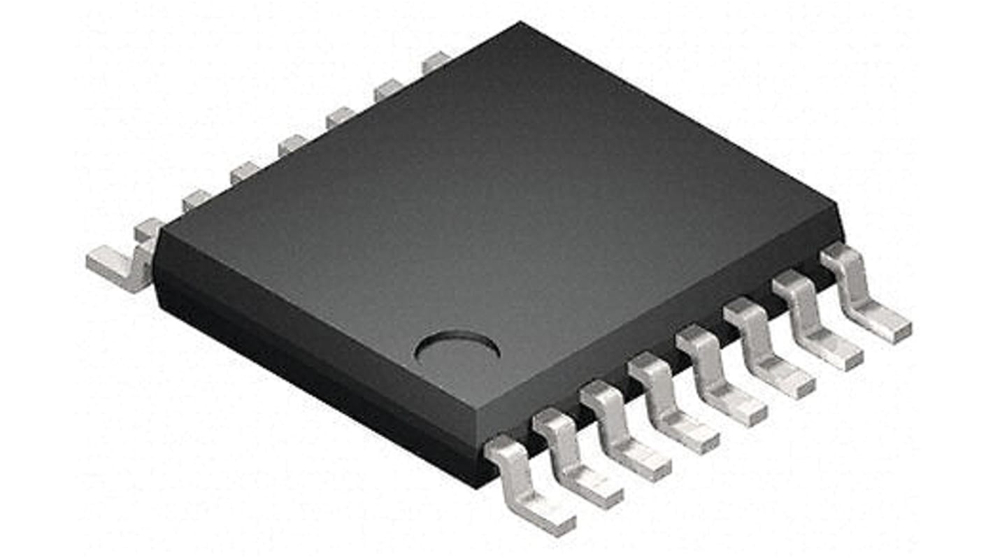
Toshiba 74VHC138FT, Decoder, 16-Pin TSSOP
- RS-stocknr.:
- 171-3433P
- Fabrikantnummer:
- 74VHC138FT
- Fabrikant:
- Toshiba

Bulkkorting beschikbaar
Subtotaal 150 eenheden (geleverd op een wiel)*
€ 32,70
(excl. BTW)
€ 39,60
(incl. BTW)
GRATIS bezorging voor bestellingen vanaf € 75,00
Op voorraad
- 3.750 stuk(s) klaar voor verzending vanaf een andere locatie
Heeft u meer nodig? Klik op 'Controleer leverdata' voor extra voorraad en levertijden.
Aantal stuks | Per stuk |
|---|---|
| 150 - 450 | € 0,218 |
| 500 - 950 | € 0,196 |
| 1000 + | € 0,178 |
*prijsindicatie
- RS-stocknr.:
- 171-3433P
- Fabrikantnummer:
- 74VHC138FT
- Fabrikant:
- Toshiba
Specificaties
Datasheets
Wetgeving en conformiteit
Productomschrijving
Zoek vergelijkbare producten door een of meer kenmerken te selecteren.
Alles selecteren | Attribuut | Waarde |
|---|---|---|
| Merk | Toshiba | |
| Mounting Type | Surface Mount | |
| Package Type | TSSOP | |
| Pin Count | 16 | |
| Dimensions | 5 x 4.4 x 1mm | |
| Maximum Operating Supply Voltage | 5.5 V | |
| Maximum Operating Temperature | +125 °C | |
| Minimum Operating Temperature | -40 °C | |
| Automotive Standard | AEC-Q100 | |
| Minimum Operating Supply Voltage | 2 V | |
| Alles selecteren | ||
|---|---|---|
Merk Toshiba | ||
Mounting Type Surface Mount | ||
Package Type TSSOP | ||
Pin Count 16 | ||
Dimensions 5 x 4.4 x 1mm | ||
Maximum Operating Supply Voltage 5.5 V | ||
Maximum Operating Temperature +125 °C | ||
Minimum Operating Temperature -40 °C | ||
Automotive Standard AEC-Q100 | ||
Minimum Operating Supply Voltage 2 V | ||
The 74VHC138FT is an advanced high speed CMOS 3-to-8 DECODER fabricated with silicon gate C2MOS technology. It achieves the high speed operation similar to equivalent Bipolar Schottky TTL while maintaining the CMOS low power dissipation. When the device is enabled, 3 Binary Select inputs (A, B and C) determine which one of the outputs ( Y0 - Y7 ) will go low. When enable input G1 is held low or either G2A or G2B is held high, decoding function is inhibited and all outputs go high. G1, G2A , and G2B inputs are provided to ease cascade connection and for use as an address decoder for memory systems. An input protection circuit ensures that 0 to 5.5 V can be applied to the input pins without regard to the supply voltage. This device can be used to interface 5 V to 3 V systems and two supply systems such as battery back up. This circuit prevents device destruction due to mismatched supply and input voltages.
Wide operating temperature: Topr = -40 to 125
High speed: Propagation delay time = 3.8 ns (typ.) at VCC = 5.0 V
Low power dissipation: ICC = 2.0 μA (max) at Ta = 25
High noise immunity: VNIH = VNIL = 28 % VCC (min)
Power-down protection is provided on all inputs.
Balanced propagation delays: tPLH ≈ tPHL
Wide operating voltage range: VCC(opr) = 2.0 to 5.5 V
Low noise: V = 0.8 V (max)