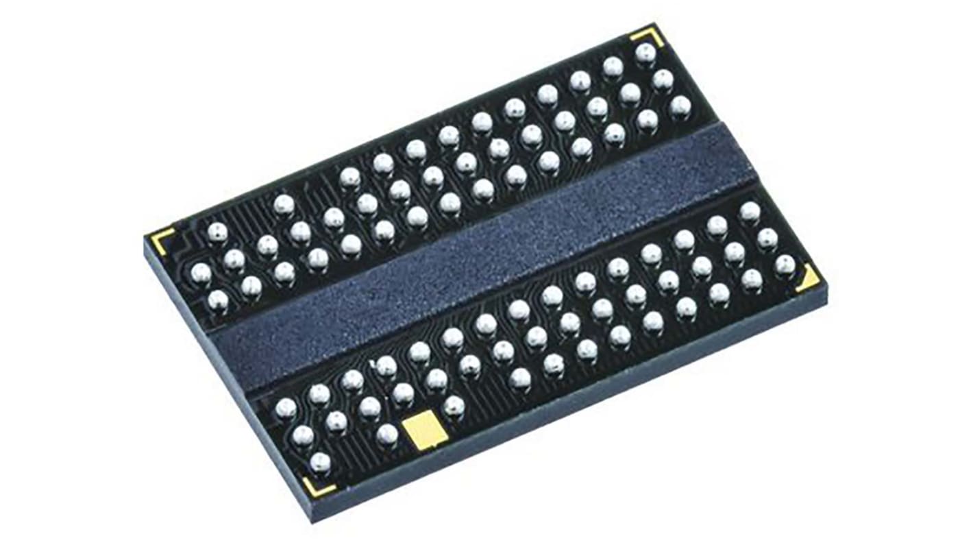
Winbond W971GG6SB25I, SDRAM 1Gbit Surface Mount, 84-Pin WBGA

- RS-stocknr.:
- 188-2756P
- Fabrikantnummer:
- W971GG6SB25I
- Fabrikant:
- Winbond
Niet meer leverbaar – bekijk hieronder eventuele alternatieven of neem contact op met onze Customer Service
- RS-stocknr.:
- 188-2756P
- Fabrikantnummer:
- W971GG6SB25I
- Fabrikant:
- Winbond
Datasheets
Wetgeving en conformiteit
- Land van herkomst:
- TW
Productomschrijving
The W971GG6SB is a 1G bits DDR2 SDRAM, and speed involving -18/18I/18J, -25/25N/25I/25J and -3.
Double Data Rate architecture: two data transfers per clock cycle
CAS Latency: 3, 4, 5, 6 and 7
Burst Length: 4 and 8
Bi-directional, differential data strobes (DQS and /DQS ) are transmitted / received with data
Edge-aligned with Read data and center-aligned with Write data
DLL aligns DQ and DQS transitions with clock
Differential clock inputs (CLK and /CLK)
Data masks (DM) for write data
Commands entered on each positive CLK edge, data and data mask are referenced to both edges of /DQS
Posted /CAS programmable additive latency supported to make command and data bus efficiency
Read Latency = Additive Latency plus CAS Latency (RL = AL + CL)
Off-Chip-Driver impedance adjustment (OCD) and On-Die-Termination (ODT) for better signal quality
Auto-precharge operation for read and write bursts
Auto Refresh and Self Refresh modes
Precharged Power Down and Active Power Down
Write Data Mask
Write Latency = Read Latency - 1 (WL = RL - 1)
Interface: SSTL_18
Specificaties
Kenmerk | Waarde |
|---|---|
| Memory Size | 1Gbit |
| Organisation | 128M x 8 bit |
| Number of Bits per Word | 8bit |
| Number of Words | 128M |
| Mounting Type | Surface Mount |
| Package Type | WBGA |
| Pin Count | 84 |
| Dimensions | 12.6 x 8.1 x 0.8mm |
| Height | 0.8mm |
| Length | 12.6mm |
| Maximum Operating Supply Voltage | 1.9 V |
| Maximum Operating Temperature | +95 °C |
| Minimum Operating Supply Voltage | 1.7 V |
| Width | 8.1mm |
| Minimum Operating Temperature | -40 °C |