Altera DK-DEV-5AGTD7N Arria V GT Development Kit 5AGTFD7K3F40I3N

- RS-stocknr.:
- 778-5354
- Fabrikantnummer:
- DK-DEV-5AGTD7N
- Fabrikant:
- Altera
Niet meer leverbaar – bekijk hieronder eventuele alternatieven of neem contact op met onze Customer Service
- RS-stocknr.:
- 778-5354
- Fabrikantnummer:
- DK-DEV-5AGTD7N
- Fabrikant:
- Altera
Wetgeving en conformiteit
Productomschrijving
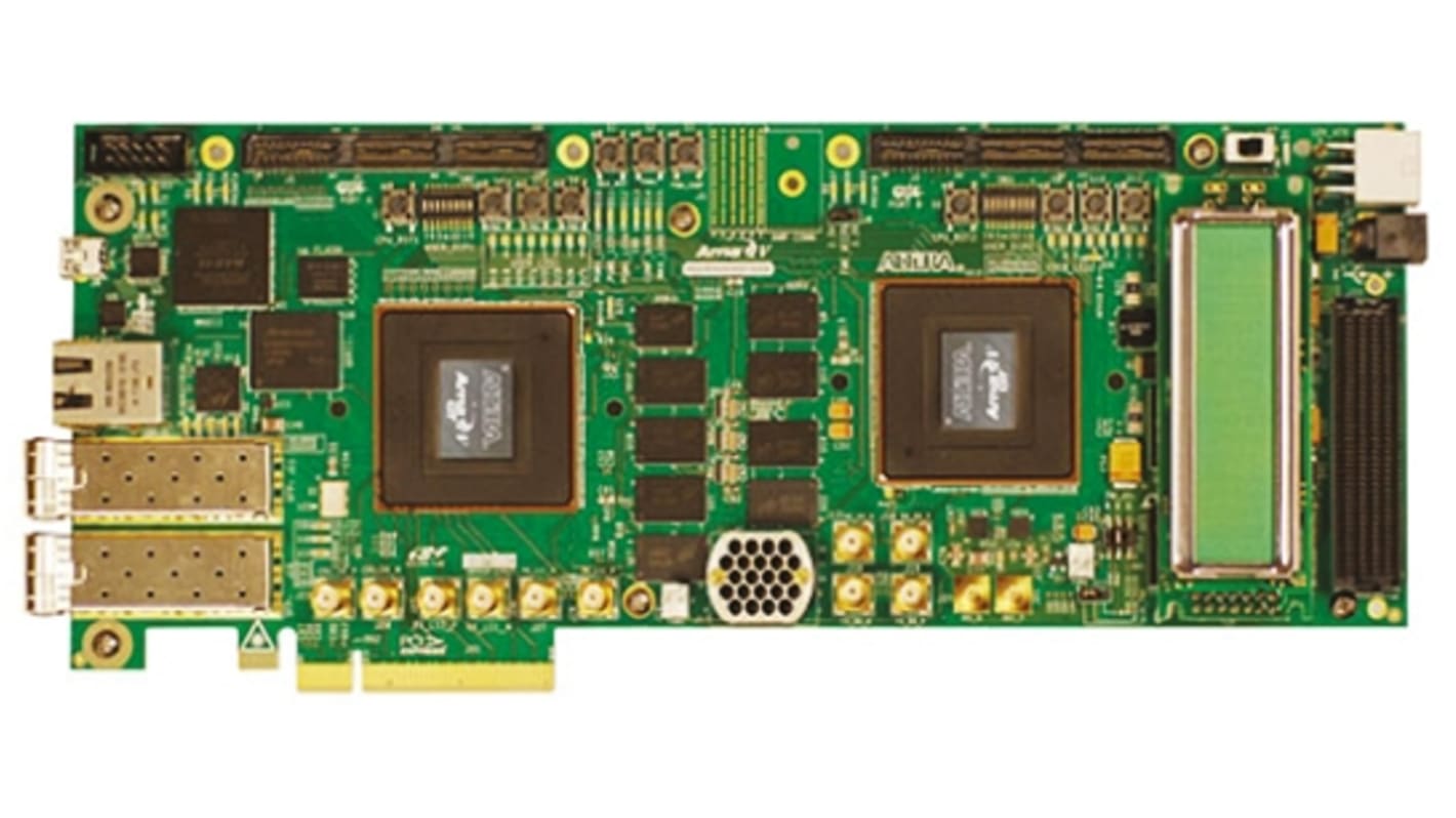
Arria V GT FPGA Development Kit, Altera
The Altera Arria® V GT FPGA Development Kit provides a complete design environment that includes all the hardware and software that you need to develop full FPGA designs and test them within a system environment.
Unit 1
Arria V GT FPGA: 5AGTFD7K3F40I3N
1152MB x 72 DDR3 SDRAM
4.5MB (1MB x 36) QDR II+ SRAM
1Gb sync Flash (x16)
PCI Express (PCIe) x8 edge connector
HSMC Port A (Eight transceiver channels)
USB 2.0
Gigabit Ethernet communication
Chip-to-chip bridge with 29 LVDS inputs, 29 LVDS outputs and x8 transceivers
2 x SFP+ channels
Bull's Eye connector (3 x 10Gbps transceiver channel)
SMA connector (10Gbps transceiver channel)
Configuration: JTAG, Fast passive parallel (FPP) parallel Flash loader (PFL)
Buttons, switches, LEDs and displays
CPU reset push button
3 x user push buttons
8 x DIP switches
16 x user LEDs (including eight bi-colour diodes)
3 x PCIe LEDs
3 x HSMA Status LEDs
2 line x 16 character LCD display
Unit 2
Arria V GT FPGA: 5AGTFD7K3F40I3N
x64 DDR3 SDRAM soft controller (or x32 hard intellectual property (IP) controller)
HSMC Port B (Four transceiver channels)
FMC Port (Ten transceiver channels)
Chip-to-chip bridge with 29 LVDS inputs and 29 LVDS outputs, and x8 transceivers
Serial digital interface (SDI) channel
Bull's Eye connector (6Gbps transceiver channel)
Bull's Eye connector (10Gbps transceiver channel)
SMA connector (10Gbps transceiver channel)
Configuration: JTAG, Fast passive parallel (FPP) parallel Flash loader (PFL)
Buttons, switches, LEDs and displays
CPU reset push button
3 x user push buttons
8 x DIP switches
16 x user LEDs (including eight bi-colour diodes)
EPM2210GF324 system controller
EPM570GM100 on-board USB-Blaster II download cable
Clocking: 50MHz and 148.5MHz oscillator
100MHz and four 4 output programmable oscillators
SMA input (LVPECL)
Power: Laptop DC input, PCIe edge connector
System monitoring, Power: (voltage, current, and wattage), per unit per rail
Arria V GT FPGA: 5AGTFD7K3F40I3N
1152MB x 72 DDR3 SDRAM
4.5MB (1MB x 36) QDR II+ SRAM
1Gb sync Flash (x16)
PCI Express (PCIe) x8 edge connector
HSMC Port A (Eight transceiver channels)
USB 2.0
Gigabit Ethernet communication
Chip-to-chip bridge with 29 LVDS inputs, 29 LVDS outputs and x8 transceivers
2 x SFP+ channels
Bull's Eye connector (3 x 10Gbps transceiver channel)
SMA connector (10Gbps transceiver channel)
Configuration: JTAG, Fast passive parallel (FPP) parallel Flash loader (PFL)
Buttons, switches, LEDs and displays
CPU reset push button
3 x user push buttons
8 x DIP switches
16 x user LEDs (including eight bi-colour diodes)
3 x PCIe LEDs
3 x HSMA Status LEDs
2 line x 16 character LCD display
Unit 2
Arria V GT FPGA: 5AGTFD7K3F40I3N
x64 DDR3 SDRAM soft controller (or x32 hard intellectual property (IP) controller)
HSMC Port B (Four transceiver channels)
FMC Port (Ten transceiver channels)
Chip-to-chip bridge with 29 LVDS inputs and 29 LVDS outputs, and x8 transceivers
Serial digital interface (SDI) channel
Bull's Eye connector (6Gbps transceiver channel)
Bull's Eye connector (10Gbps transceiver channel)
SMA connector (10Gbps transceiver channel)
Configuration: JTAG, Fast passive parallel (FPP) parallel Flash loader (PFL)
Buttons, switches, LEDs and displays
CPU reset push button
3 x user push buttons
8 x DIP switches
16 x user LEDs (including eight bi-colour diodes)
EPM2210GF324 system controller
EPM570GM100 on-board USB-Blaster II download cable
Clocking: 50MHz and 148.5MHz oscillator
100MHz and four 4 output programmable oscillators
SMA input (LVPECL)
Power: Laptop DC input, PCIe edge connector
System monitoring, Power: (voltage, current, and wattage), per unit per rail
Supplied with
Loopback and debug HSMC cards, Samtec's Bull's Eye assembly kit, cables, documentation, software
An FPGA is a semiconductor device consisting of a matrix of Configurable Logic Blocks (CLBs) connected through programmable interconnects. The user determines these interconnections by programming SRAM. A CLB can be simple (AND, OR gates, etc) or complex (a block of RAM). The FPGA allows changes to be made to a design even after the device is soldered into a PCB.
Specificaties
Kenmerk | Waarde |
|---|---|
| Programmable Logic Technology | FPGA |
| Kit Classification | Development Kit |
| Featured Device | 5AGTFD7K3F40I3N |
| Kit Name | Arria V GT |
- RS-stocknr.:
- 778-5354
- Fabrikantnummer:
- DK-DEV-5AGTD7N
- Fabrikant:
- Altera